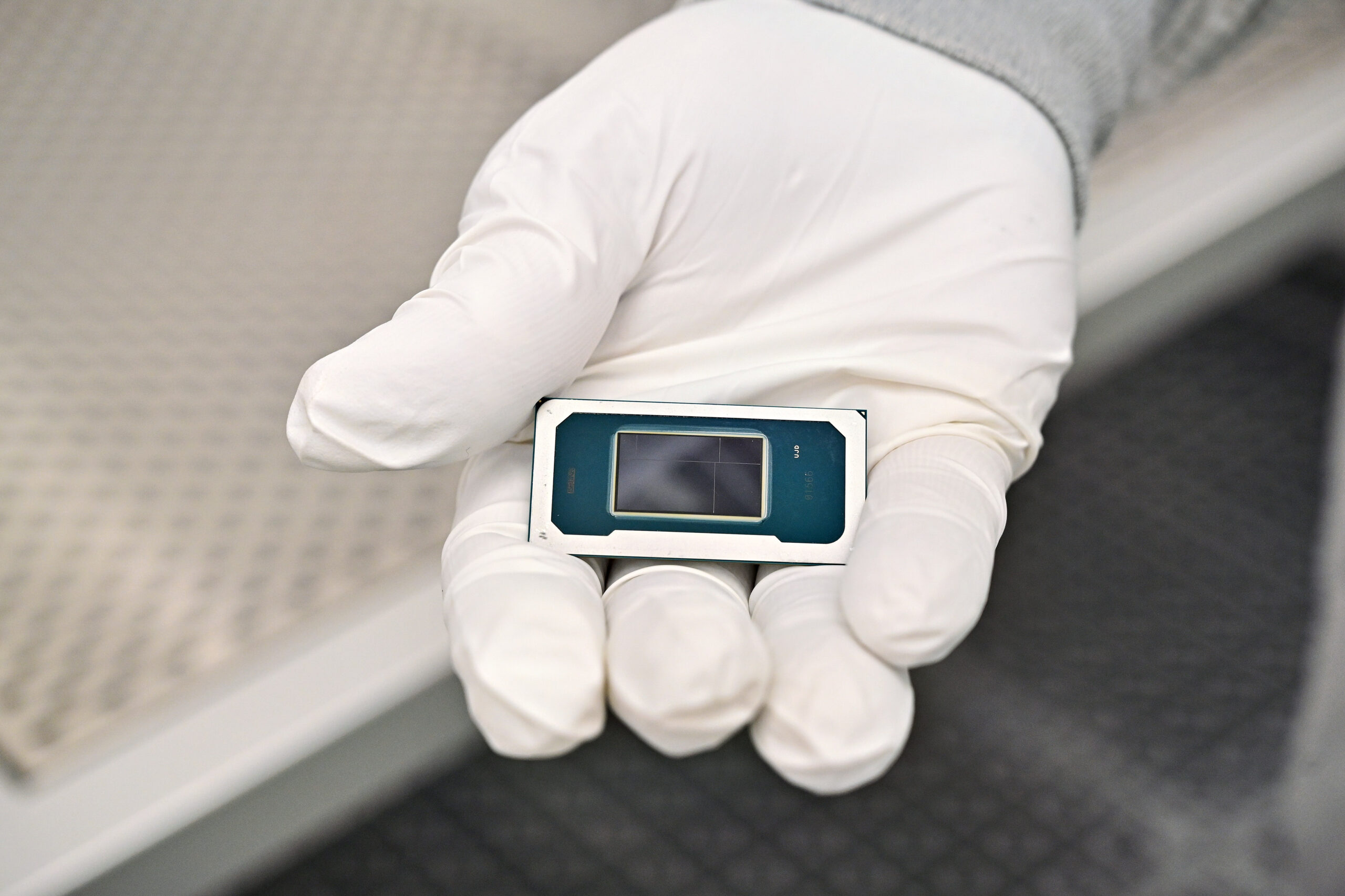
TECH – Intel has taken a major step toward the next generation of semiconductor manufacturing by successfully integrating High Numerical Aperture Extreme Ultraviolet (High-NA EUV) lithography into preparations for high-volume production of its upcoming Panther Lake processors. According to Interesting Engineering, the milestone reinforces Intel’s strategy to regain manufacturing leadership through cutting-edge chip fabrication technologies capable of producing smaller, faster, and more energy-efficient processors.
High-NA EUV is regarded as one of the most advanced chipmaking technologies ever developed. Built by Dutch equipment manufacturer ASML, the system uses an upgraded optical design with a higher numerical aperture, enabling semiconductor manufacturers to print much finer circuit patterns onto silicon wafers. Compared with conventional EUV machines, the new technology offers significantly greater precision, reducing the number of manufacturing steps required while improving production efficiency and chip performance.
According to Interesting Engineering, Intel has become the first major semiconductor company to publicly demonstrate High-NA EUV systems operating as part of its manufacturing workflow. The technology is expected to play a crucial role in producing Panther Lake processors, which are scheduled for future commercial release. By simplifying complex lithography processes, Intel aims to increase manufacturing yields while lowering production costs for advanced semiconductor devices.
The company also reported encouraging results from its early production testing, indicating that High-NA EUV has met performance expectations during pilot manufacturing. Engineers believe the improved imaging capabilities will allow future processors to contain even more transistors within the same chip area, leading to higher computing performance, greater energy efficiency, and stronger artificial intelligence processing capabilities.
Read More: MIT Robot Swims and Flies Like a Diving Seabird Naturally
Discussing the achievement, Intel executives emphasized the importance of moving advanced research into large-scale manufacturing. “We are bringing High-NA EUV into high-volume manufacturing,” the company stated, describing the transition as a significant milestone for the semiconductor industry. The announcement highlights Intel’s long-term commitment to investing in next-generation manufacturing technologies that can support increasingly complex processor designs.
Beyond Panther Lake, High-NA EUV is expected to influence future generations of processors across personal computers, data centers, artificial intelligence systems, and high-performance computing applications. As transistor dimensions continue shrinking, advanced lithography will become increasingly essential for sustaining improvements predicted by Moore’s Law.
Looking ahead, as reported by Interesting Engineering, Intel’s progress demonstrates that High-NA EUV is moving from experimental development toward practical industrial deployment. While further optimization remains necessary before full-scale commercialization, the successful integration of this groundbreaking lithography technology represents an important advance in global semiconductor manufacturing, positioning Intel to compete more aggressively in the race to produce the world’s most advanced computer chips.