TECH – Huawei’s newly surfaced Kunpeng 930 server chip is generating buzz over its advanced chiplet architecture and the mystery surrounding its foundry origins. A teardown leak, now highlighted by TrendForce, hints at a hybrid manufacturing strategy—integrating compute dies produced with TSMC’s 5nm node and an I/O die possibly made using SMIC’s more mature process.
According to insiders and teardown analysis shared via X by user @Kurnalsalts and covered by Wccftech and TechPowerUp, the Kunpeng 930 contains multiple dense compute tile chiplets manufactured with TSMC’s 5nm (N5) technology, alongside a significantly larger I/O die, speculated to be fabricated on SMIC’s 14nm node. This strategic combination allows Huawei to harness the high performance and SRAM density benefits of N5 while managing volume and supply constraints by offloading I/O functions to a locally accessible process.
Complicating the picture, sources like NetEase News and MyDrivers propose that SMIC’s advanced N+3 process might serve as the manufacturing platform—offering transistor densities between TSMC’s N6 and Samsung’s 5nm, roughly akin to TSMC’s 5.5nm level.
Read More: Honor Magic V5 Brings Real-Time On-Device AI Call Translation
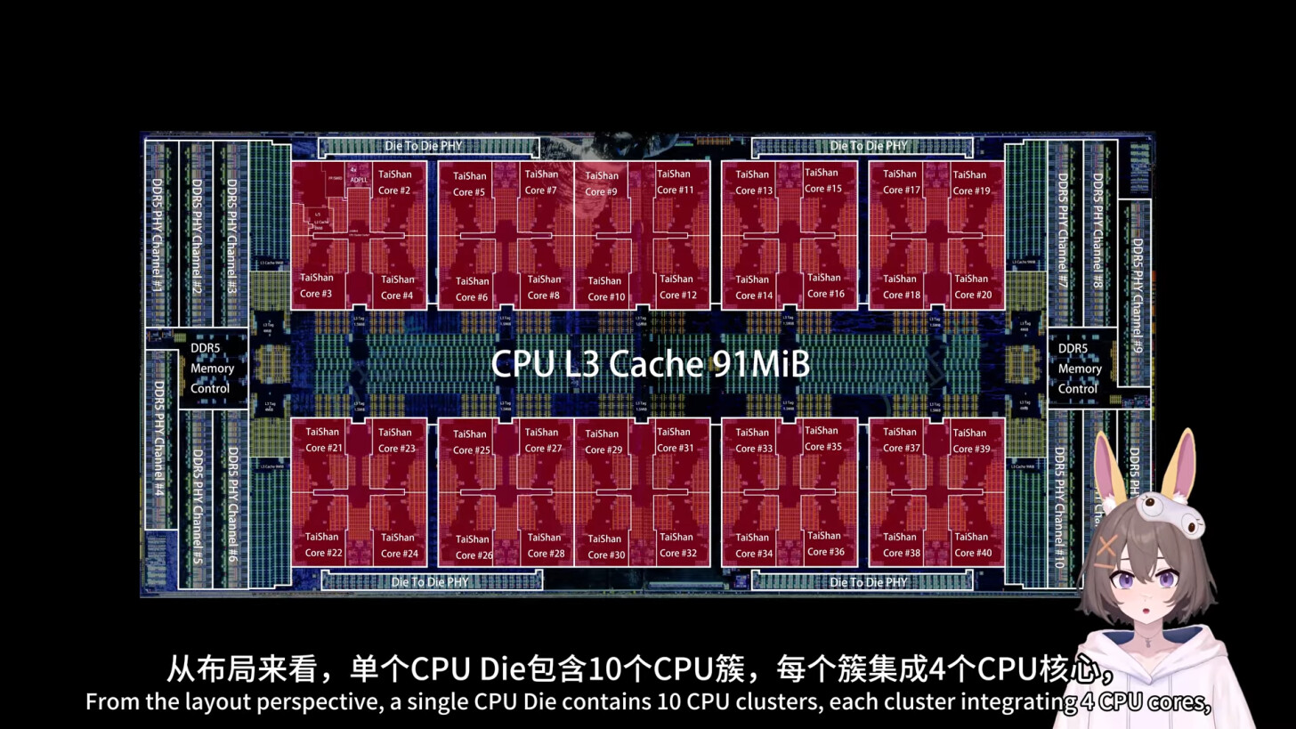
Further teardown revelations shed light on the chip’s scale and specifications: the Kunpeng 930’s footprint measures approximately 77.5 mm × 58.0 mm, featuring four compute chiplets (~252.3 mm² each) plus one large I/O die (~312.3 mm²), making its I/O die about 81.3% larger than its predecessor’s. The processor boasts 120 cores based on Huawei’s ARM-derived “Mount TaiShan” architecture, with each die containing 2 MB of L2 cache and sharing a total of 91 MB L3 cache.
On the connectivity front, the chip supports 96 PCIe lanes, 16-channel DDR5 memory, and is designed for dual-socket motherboard configurations, enabling dual-CPU deployments for high-performance server applications.
This leak raises critical questions about Huawei’s strategic approach amid geopolitical constraints. Blending advanced TSMC manufacturing for performance-critical compute components with locally feasible SMIC nodes for I/O could offer Huawei a pathway to stay competitive under U.S. technology embargoes. However, whether the input die is indeed produced by SMIC—and if so, under which node—remains speculative.
As sanctions continue to restrict access to leading-edge lithography, this hybrid chiplet design might become a template for confronting supply challenges and ensuring technological progress. Confirmation of SMIC’s role in fabricating the I/O die could mark a significant milestone in China’s semiconductor self-reliance strategy.
Source: trendforce.com